Chips to Start-up Programme: Building India’s Indigenous Chip Design Ecosystem
Context
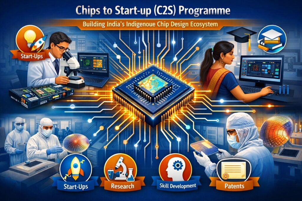
The Chips to Start-up (C2S) Programme is in the spotlight for delivering concrete results such as 56 student-designed chips fabricated, 75+ patents filed, and massive chip design training, signalling India’s steady progress toward an indigenous semiconductor design ecosystem.
Programme Snapshot: A national capacity-building and innovation initiative designed to produce industry-ready semiconductor professionals by combining academic learning with real-world chip design and fabrication exposure.
Launch & Nodal Agency: Launched in 2022 by the Ministry of Electronics and Information Technology (MeitY).
Primary Objective: To build a strong talent pipeline in chip design, facilitate hands-on silicon development, promote start-ups and IP generation, and enhance technological self-reliance in semiconductors.
Financial Framework: ₹250 crore allocation over five years.
Human Capital Targets: Training of 200 PhDs, 7,000 M.Tech (VLSI), 8,800 M.Tech (allied disciplines with VLSI exposure), and around 69,000 B.Tech students.
Infrastructure & Tool Access: Nationwide access to shared EDA tools, high-performance computing (HPC), FPGA boards, and SMART laboratories.
Fabrication & Validation: Shared wafer fabrication runs through the Semi-Conductor Laboratory (SCL), Mohali, enabling students to translate designs into actual silicon.
Institutional Support: The National ChipIN Centre, operated by C-DAC, Bengaluru, providing end-to-end support for chip design, prototyping, and validation.
Industry Integration: Training and mentoring in collaboration with global EDA vendors and semiconductor firms, ensuring alignment with industry standards.
Key Features
End-to-end learning: Covers the entire chip lifecycle from design to fabrication and testing.
Shared national infrastructure: Reduces entry barriers by democratising access to advanced tools.
Start-up and IP focus: Encourages patents, IP cores, ASICs, and SoCs.
Scalable talent creation: Targets students across UG, PG, and PhD levels.
Importance
Addresses skill shortages: Helps bridge the global and domestic semiconductor skill gap.
Supports Atmanirbhar Bharat: Strengthens self-reliance in a strategic and security-sensitive sector.
Boosts innovation ecosystem: Links academia, industry, and start-ups in chip design.
Reduces import dependence: Lays the foundation for domestic design capabilities complementing fabrication initiatives.
Source :PIB