
NITI Aayog Unveils India Semiconductor Vision 2035 Roadmap
Context
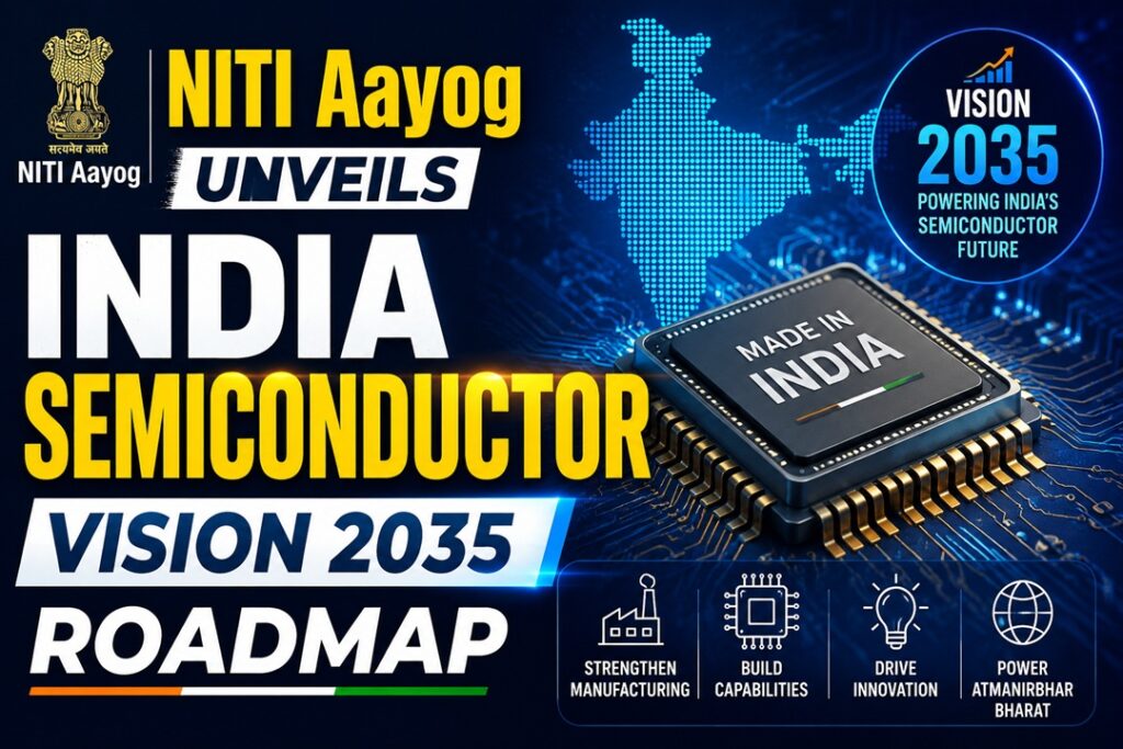
NITI Aayog’s Frontier Technologies Division has unveiled a long-term strategic blueprint titled “India Semiconductor Vision 2035”, outlining a comprehensive pathway to establish India as a globally competitive semiconductor manufacturing and innovation hub.
India Semiconductor Vision 2035
About the Roadmap
What is it?
The India Semiconductor Vision 2035 is a strategic framework designed to create a domestic semiconductor ecosystem valued at USD 120–150 billion by 2035. Instead of directly competing in the capital-intensive race for cutting-edge wafer fabrication, the roadmap emphasizes a differentiated growth model.
It promotes a “Smart Specialization Strategy”, focusing on mature-node manufacturing, advanced semiconductor packaging, chip design innovation, and next-generation compound semiconductors such as silicon carbide (SiC) and gallium nitride (GaN).
Major Observations of the Report
Heavy Import Dependence
India continues to rely on overseas suppliers for nearly 90–95% of its semiconductor requirements, exposing critical sectors to external disruptions.
Rapid Expansion of Domestic Demand
Growing electronics production, electric mobility adoption, AI infrastructure, and digitalization are expected to drive India’s semiconductor demand to nearly USD 200 billion by 2035.
Large Foreign Exchange Burden
Substantial dependence on imported chips has generated a cumulative import expenditure of approximately USD 150 billion during FY17–FY25.
Rising Import Exposure
Without domestic manufacturing expansion, semiconductor imports could rise to nearly USD 240 billion annually by 2035.
Strong Design Ecosystem
India hosts nearly 20% of the global semiconductor design talent pool, providing a strong foundation for indigenous innovation.
Significant Investment Requirement
Developing fabrication facilities, packaging units, research centers, and supply-chain infrastructure may require investments of USD 135–180 billion over the coming decade.
Global Market Participation Goal
The roadmap envisions India securing 10–13% of global semiconductor value-chain participation by 2035.
Shift Towards Advanced Capability Building
Under the next phase of the India Semiconductor Mission (ISM), policy focus is expected to move from capacity creation toward strengthening R&D, design IP, and advanced manufacturing capabilities.
Growth Drivers for India’s Semiconductor Sector
Transforming Design Strength into Product Innovation
India’s vast engineering workforce can transition from service-oriented chip design activities toward creating globally marketable semiconductor intellectual property.
Example: The roadmap aims to facilitate the creation of over 100 advanced indigenous semiconductor IPs by 2035.
Benefiting from Supply-Chain Diversification
Global efforts to diversify semiconductor supply chains beyond traditional manufacturing centers present India with a strategic opportunity.
Example: Enhanced partnerships with the US, Japan, South Korea, and Europe can strengthen India’s integration into trusted technology ecosystems.
Growing Demand from Automotive Electrification
Electric vehicles and intelligent mobility systems require increasing volumes of power electronics and specialized chips.
Example: Domestic demand can support manufacturing of SiC and GaN-based semiconductor components for EV applications.
Leadership in Advanced Packaging Technologies
Advanced packaging offers a cost-effective alternative to competing in leading-edge fabrication technologies.
Example: India aims to emerge among the leading global centers for OSAT services, chiplet integration, and 3D packaging solutions.
Strengthening Strategic Self-Reliance
Domestic semiconductor manufacturing can enhance security and reduce dependence in sectors such as defense, telecommunications, and critical infrastructure.
Key Challenges Highlighted
High Capital Intensity
Semiconductor fabrication remains one of the most expensive manufacturing activities globally.
Example: Advanced fabrication plants can require investments exceeding USD 15 billion, while even mature-node facilities demand several billion dollars.
Long Project Timelines
Semiconductor facilities require extended periods for construction, calibration, and yield optimization before becoming commercially viable.
Shortage of Specialized Manufacturing Skills
Although India possesses strong software and design expertise, there remains a shortage of professionals trained in fabrication processes, materials science, and advanced packaging.
Resource-Intensive Operations
Chip manufacturing requires reliable access to ultra-pure water, uninterrupted electricity, and high-quality industrial infrastructure.
Example: Semiconductor fabs consume massive quantities of purified water and significant energy resources.
Established Global Competition
Existing semiconductor hubs in East Asia benefit from mature ecosystems, supplier networks, and longstanding customer relationships, creating entry barriers for new entrants.
Strategic Recommendations
Launch a Semiconductor Growth Fund
The government should provide long-term public capital support, risk-sharing mechanisms, and financial incentives to attract large-scale investments.
Develop Dedicated Semiconductor Manufacturing Clusters
Establish specialized industrial regions equipped with world-class utilities, logistics networks, and research facilities.
Integrate AI into Chip Development
Leverage artificial intelligence and advanced Electronic Design Automation (EDA) tools to accelerate semiconductor design and reduce development costs.
Promote Domestic Procurement
Encourage adoption of domestically produced chips across government-backed sectors including railways, defense, telecommunications, and smart infrastructure.
Create a National Semiconductor Skills Network
Develop dedicated institutions and industry partnerships to train fabrication engineers, process specialists, packaging experts, and equipment technicians.
Conclusion
India Semiconductor Vision 2035 represents a strategic transition from building foundational capacity to establishing deep technological capabilities. By emphasizing advanced packaging, mature-node production, design leadership, and skill development, the roadmap seeks to position India as a resilient and globally significant player in the semiconductor value chain while capitalizing on its existing engineering strengths.
Source: PIB